Tutorials
This a simple guide that will help you with the processes of generating your Gerber files using either Altium Design software or Eagle.
How to properly export the gerber files, parts-centroid file (pick&place file) and BOM from Altium Designer Software?
A Gerber file for each section of your electronic circuit design is what you need if you want to create a PCB. Watch the video from myProto youtube channel to get to know how to generate the required files for myProto platform.
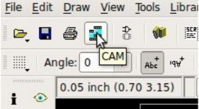
In Eagle, open Board view. Click the CAM button or choose “File -> CAM Procesor”.
This will open the CAM Processor tool that is used to generate the files. Here you can define the sections you want to create files for.
To simplify creating Gerber files, you can use the predefined job of myProto. This is the file myProto RS-274x 2layers.cam for two-layer circuits and the file myProto RS-274x 4layers.cam for four-layer circuits.
We recommend that you put these two files in the directory C:\EAGLE-x.x.x\cam
To open it in the CAM Processor click “File -> Open -> Job”
Browse to your /eagle/cam/ folder, and you should see a file called. Choose it and click “Open”.
You will now see several tabs in the CAM Processor. Each of these tabs will generate a Gerber file.
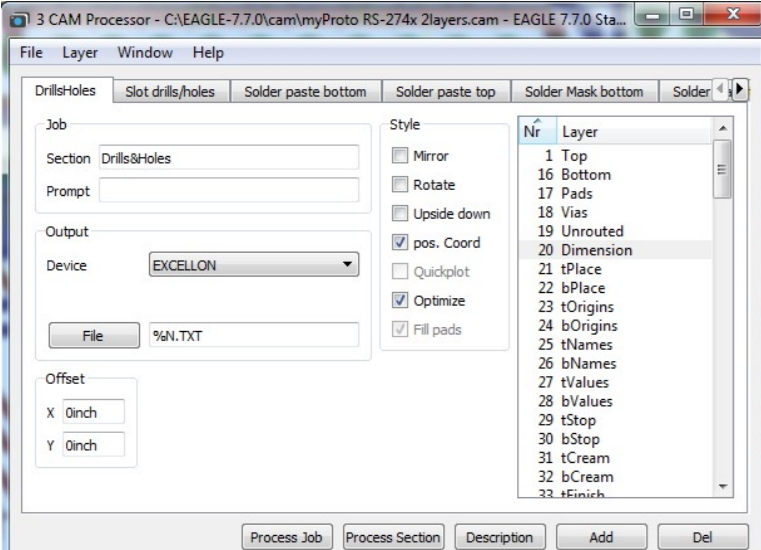
Click on “Process Job” to output the Gerber files.
You will find the files in your project directory folder.
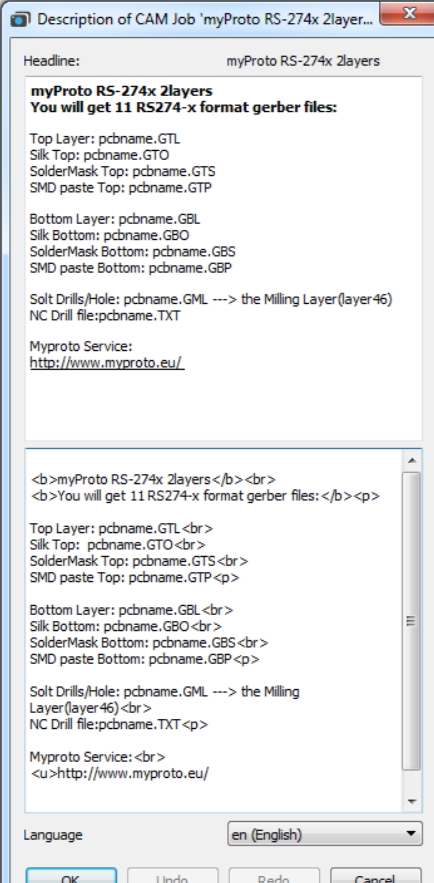
You will get 10 RS274-x format gerber files with myProto RS-274x 2 layers:
Upload your file and get a preview of your PCB in our online gerber viewer. Inspect the individual layers and view your PCB layout everywhere you would like. This is an online gerber viewer that doesn’t store your Gerber file on any server.
Get in touch with our support team. We will contact you within the next 24hours.
Member of